SpaceConstrainedStabilizerDiodeSeriesForModernPCBDesign
When you’re squeezing a 12‑layer board into a rugged IoT gateway housing, the usual suspects—bulky axial Zeners or oversized SOT‑23 packages—start looking like liabilities. You need something that sits quietly on the board, survives automotive temperature swings, and doesn’t fight your pick‑and‑place line. That’s where the PD3Z284C series steps in: a family of 0.5 W surface‑mount Zener diodes built for exactly these tight‑corner scenarios.
The planar die construction isn’t just a marketing bullet—it translates to consistent breakdown characteristics across the full –65 °C to +150 °C range, which matters when your design ends up in both factory floors and vehicle engine bays. The PowerDI323 (Type B) package is tiny enough to tuck next to a sensitive analog front‑end without crowding routing channels, yet it still meets AEC‑Q101 for reliability. If you’ve ever had a “small” diode fail during ESD testing, you’ll appreciate the fully lead‑free, halogen‑free build that doesn’t compromise on robustness.
In practice, I’ve found these diodes particularly useful in two spots: protecting RS‑485 bus lines from transient spikes and providing stable reference voltages for low‑power ADCs. For the 5 V bus protection, the PD3Z284C5V1 (with its 4.8–5.4 V window) clamps nicely without interfering with normal signaling. When you need a quiet reference for a 12‑bit ADC, the PD3Z284C3V3 offers a tight 3.1–3.5 V range with minimal temperature drift—just watch your thermal layout, because even 500 mW can heat a small package quickly.
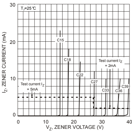
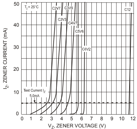
The marking codes follow a simple logic: two‑character IDs that map directly to nominal voltages. For example, “0K” means 6.2 V, and “12” corresponds to 24 V. This makes visual inspection straightforward during rework—no need to cross‑reference long part numbers under a microscope.
| Nominal Zener Voltage (V) | Marking Code | Min Vz (V) | Max Vz (V) | Zzt @ IzT (Ω) | Temp Coeff (mV/°C) |
|---|---|---|---|---|---|
| 2.4 | 06 | 2.20 | 2.60 | 100 | –3.5 to 0 |
| 3.3 | 0B | 3.10 | 3.50 | 95 | –3.5 to 0 |
| 5.1 | Z0G, 0G | 4.80 | 5.40 | 60 | –2.7 to 1.2 |
| 6.2 | Z0K, 0K | 5.80 | 6.60 | 10 | 0.4 to 3.7 |
| 12 | Z0S, 0S | 11.4 | 12.7 | 10 | 6.0 to 10.0 |
| 24 | 12 | 22.8 | 25.6 | 30 | 18.4 to 22.0 |
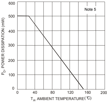
One practical tip: if your application runs near the upper end of the voltage range, double‑check the thermal resistance. With RθJA at 250 °C/W, a few hundred milliwatts of dissipation can push junction temperatures higher than you expect. I usually add a small copper pour under the pad for anything above 200 mW continuous—nothing fancy, just enough to keep things cool without complicating the layout.
For selection, start with your worst‑case operating voltage and work backward. If you need a 3.3 V rail clamp, don’t just grab the 3.3 V diode—consider the tolerance and temperature coefficient. In noisy environments, the tighter‑tolerance parts (like the 5.1 V or 6.2 V variants) often save you debugging time later.
These diodes won’t win awards for flashy features, but they solve real problems in compact, high‑reliability designs. Whether you’re building industrial sensors, automotive modules, or space‑constrained consumer gear, having a dependable, tiny Zener family in your library is one less thing to worry about when the schedule gets tight.